
Are you ever in the situation of modeling the AC current distribution within conductors that are connected to lumped circuit elements such as capacitors, resistors, and inductors — but you do not want to model these lumped circuit elements explicitly? If so, there is a set of features in the AC/DC Module that can help connect a full-fidelity volumetric model of a conductor to an approximate, or lumped, model of a circuit element. Let’s find out how to do so!
Model Setup for a Circuit Board with Copper Traces and Capacitors
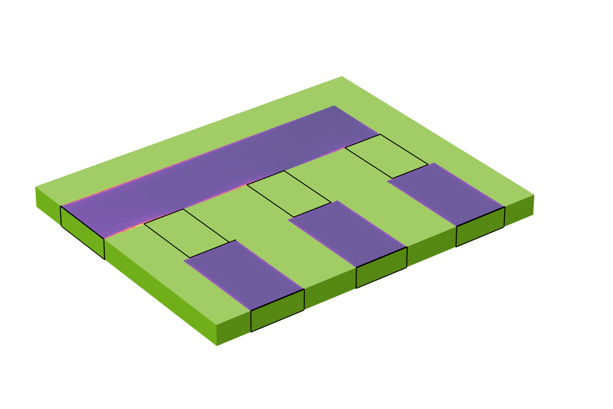
Suppose that you have a 1.5-mm-thick printed circuit board (PCB), consisting of a dielectric that is sandwiched between a conducting base layer and a 200-µm-thick copper pattern at the top. On this board there are several surface mount capacitors soldered between the traces of the top layer, as pictured below. One of the traces is excited, and due to the difference in the capacitance of the three capacitors, the signal will be split up between the outputs. At operating frequencies around 100 kHz, the skin depth will be comparable to the copper thickness, and thus we should model both the volume of the copper conductors as well as the volume of the dielectric and air to correctly capture the behavior of the transmission line. (For more details about modeling transmission lines, see our Learning Center article “Modeling TEM and Quasi-TEM Transmission Lines”.) For the purposes of this model, we do not want to include a detailed model of the surface mount capacitors; we simply want to introduce an additional capacitive coupling between the transmission lines to see what happens to the applied signal.
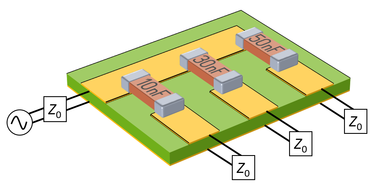
A modeled section of a PCB with a 200-µm-thick ground plane and copper traces with three surface mount capacitors. The remainder of the board is not modeled, and the traces are transmission lines of known impedance.
Since there are significant skin and proximity effects within the conductors, using the Magnetic Fields interface is appropriate. To model the capacitors within this interface, we use the Lumped Element feature and set the type to User defined. This feature should be applied to a rectangular face that bridges the gap across the area where we want to introduce the lumped component. This face needs to be sketched within the geometry sequence.
We will need to specify three geometry-based inputs in the Lumped Element feature. The lumped element direction should be a vector that points parallel to the direction between the conductors (shown below). That is, we will define that the current in the device is, in an averaged sense, flowing parallel to this vector. The lumped port height is the distance across the gap between the conductive domains; it is used to integrate the electric field and evaluate the electric potential drop across the device. The lumped port width is the orthogonal direction of the rectangular face.
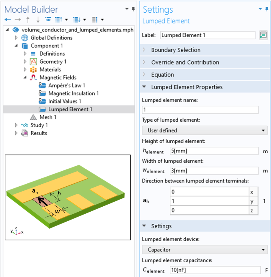
A screenshot of the Lumped Element feature with the User defined type option selected and the lumped port height, width, and direction specified.
Along with the geometric lumped element information, we need to specify the frequency-dependent impedance of the element. We can switch between the built-in options for a User defined, Capacitor, Inductor, Parallel LC, Series LC, Parallel RLC, and Series RLC equivalent impedance. The User defined option allows for a frequency-dependent, complex-valued expression. Doing so allows an arbitrary equivalent circuit to be added into a frequency-domain model.
With respect to the excitation of this model, we want to simulate four transmission lines of known impedances connected between the traces and ground plane. To do this we can use the Lumped Port feature and set the type to User defined. The Lumped Port feature is nearly identical to the Lumped Element feature in usage and functionality, differing only in that it allows an excitation to be applied and the S-parameters to be monitored.
The type of lumped port can also be set to Circuit, which allows for an arbitrarily complicated combination of lumped circuit elements to be introduced into the model via the Electrical Circuit interface. For a frequency-domain model, using the Circuit type is functionally identical to using a Lumped Element feature with a frequency-dependent impedance that is User defined. On the other hand, for a time-domain model, you will need to use the Electric Circuit interface to add lumped capacitances or inductances.
In terms of the setup, we need to be aware of the boundary conditions of our model. We are only modeling a small section of the board and transmission lines and will assume that the surroundings do not affect the behavior; that is, we will ignore any crosstalk from surrounding structures. We choose to place our model within a larger air box with Perfect Magnetic Conductor boundary conditions along the outside, simulating an insulative enclosure. For a further discussion on this, see our blog post “How to Choose Between Boundary Conditions for Coil Modeling”.
Evaluating the Results
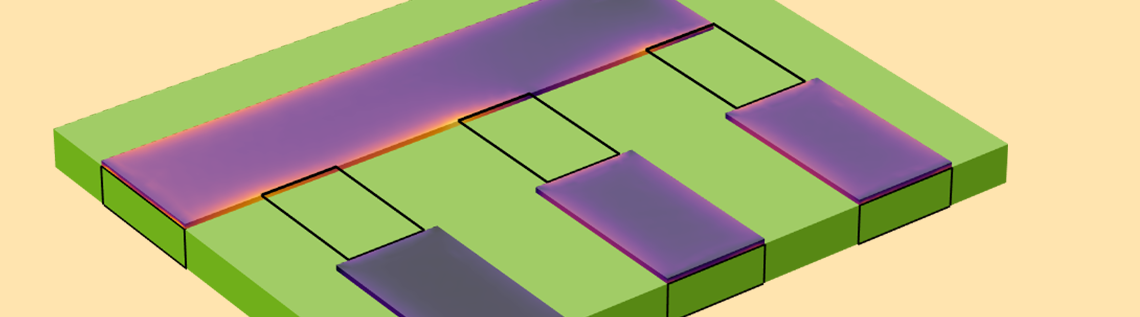
After solving this model at an operating frequency of 100 kHz, we can evaluate the S-parameters and plot the currents in the conductors as shown in the image below. Observe the skin effect and the splitting of the current based upon the magnitude of the capacitive coupling introduced by the lumped elements. This verifies that we have introduced a current path into our model across the lumped element surfaces.
A plot of the currents within the volume of the conductive traces.
Solving at Higher Frequencies
Now let’s consider what happens if the operating frequency is increased to 10 MHz, for example. At this frequency, the skin depth is about one tenth of the trace thickness, so it is no longer necessary to model the interior volume of the copper traces. We can instead use the Impedance Boundary Condition on all of the boundaries of the copper. For more details on why this is reasonable to do, see our blog post “How to Model Conductors in Time-Varying Magnetic Fields”. By solving for the magnetic fields only within the air and the dielectric, we solve a problem with fewer total degrees of freedom. It is now possible to switch the lumped ports and lumped elements from a User defined type to a Uniform type. Since the faces where these boundaries are applied are now bounded on two sides by a conductive boundary, the Uniform type setting will automatically determine the port width, height, and direction.
At higher frequencies, the interiors of the conductors do not need to be modeled, and the Impedance Boundary Condition can be used so that currents flow on the surfaces of the conductors.
Solving Thinner Layers of Conductors
To close out this discussion, let’s look at how to model a thinner copper trace. As the thickness of the trace is reduced, the resultant elements used to mesh the thickness become smaller, and this increases the computational cost. We can avoid a geometric model of the trace thickness by instead using the Transition Boundary Condition, which can be applied on interior boundaries, i.e., boundaries where the fields are solved for on either side. This allows us to model the trace as a boundary of zero geometric thickness, which further reduces the degrees of freedom in the model — although we may want a slightly finer mesh on the trace itself. The capacitive effects due to the finite height of the trace are not included in such a model, but it is reasonable to assume that they are small.
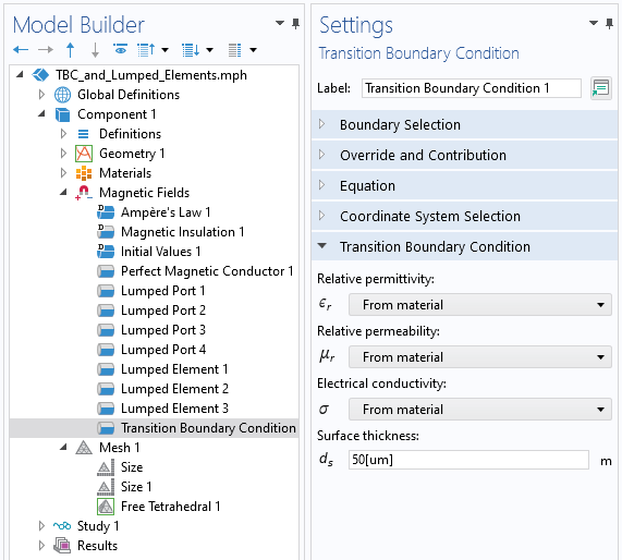
A screenshot of the Transition Boundary Condition, which computes the loss on interior boundaries based upon the material properties and the thickness.

The results of using the Transition Boundary Condition. Currents are flowing on a surface of zero geometric thickness.
Closing Remarks
We have covered here how to use the Lumped Element feature to model an equivalent circuit element in conjunction with a model of a solid conductor. We then extended the discussion to include two more cases: a solid conductor modeled via the Impedance Boundary Condition when the skin depth is very small and a very thin solid modeled via the Transition Boundary Condition — all in combination with lumped elements. These modeling techniques are useful to anyone modeling circuit boards or otherwise wanting to include lumped circuit elements in their electromagnetics models. It is worth mentioning that all of these techniques can be used within the Electromagnetic Waves, Frequency Domain formulation of the RF Module, not just the Magnetic Fields formulation of the AC/DC Module.


Comments (0)