Simulation Based Characterization of CdS Thin Film Transistor
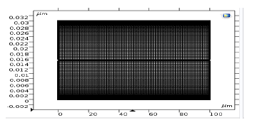
Current vs. voltage characteristics simulations of field effect transistors based on CdS semiconductor have been carried out using the drift-diffusion model. In the present investigation, the two-dimensional device simulation was performed using COMSOL’s semiconductor module. The device was designed with 80 m channel length and width. A drift-diffusion (DD) simulation model was used in which the basic equations taken are similar to those used for a single-crystal device except that traps and defects are included in the model. It is assumed that traps due to grain boundaries are uniformly distributed throughout the film. Both exponential and Gaussian trap distributions have been introduced in the simulation. The simulation was in good agreement with experiment.
Herunterladen
- wondmagegn_poster.pdf - 0.4MB
- wondmagegn_abstract.pdf - 0.01MB