Die Application Gallery bietet COMSOL Multiphysics® Tutorial- und Demo-App-Dateien, die für die Bereiche Elektromagnetik, Strukturmechanik, Akustik, Strömung, Wärmetransport und Chemie relevant sind. Sie können diese Beispiele als Ausgangspunkt für Ihre eigene Simulationsarbeit verwenden, indem Sie das Tutorial-Modell oder die Demo-App-Datei und die dazugehörigen Anleitungen herunterladen.
Suchen Sie über die Schnellsuche nach Tutorials und Apps, die für Ihr Fachgebiet relevant sind. Beachten Sie, dass viele der hier vorgestellten Beispiele auch über die Application Libraries zugänglich sind, die in die COMSOL Multiphysics® Software integriert und über das Menü File verfügbar sind.
This model and tutorial demonstrates the use of an Application Method to compute and plot the geometric Modulation Transfer Function (MTF) for the Petzval Lens. Mehr lesen

This model demonstrates how to simulate surface plasmon polaritons in a thin metal layer embedded in dielectric layers. It calculates the dispersion and propagation length of surface plasmon polaritons as a function of photon energy. Mehr lesen

This tutorial shows how to set up a multi-element objective lens. The chosen lens is the Double Gauss described in 'Modern Lens Design (2nd edition)', by W. Smith, 2005, pg 323. The tutorial demonstrates how to create a geometry sequence using the 'Spherical Lens 3D' part found in the ... Mehr lesen

This tutorial shows how to set up a multi-element objective lens. The chosen lens is a Petzval lens with field flattener described in 'Fundamental Optical Design', by M. Kidger, 2001, pg 192. The tutorial demonstrates how to include a geometric sequence using the 'Spherical General Lens ... Mehr lesen

This example demonstrates how to optimize the thickness of a microelectromechanical systems (MEMS) mirror coating material for maximum reflectivity. To reduce the simulation time, a Layered Impedance Boundary Condition is used to model the thin coating material on top of the metallic ... Mehr lesen

This model includes a dielectric slab waveguide with a small lossy metallic object nearby. The object causes light to be scattered, absorbed, and both reflected and transmitted along the waveguide. Learn more in this accompanying blog post: Modeling a Scatterer Near an Optical Waveguide Mehr lesen
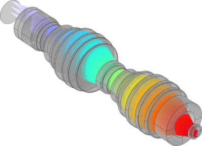
Microlithography lenses are used to project the image of an integrated circuit onto a silicon substrate. This tutorial demonstrates how to create a 21-element fused silica lens which has a NA of 0.56 which is designed to be used at a wavelength of 248nm. The lens, which has a total ... Mehr lesen

This example shows how to perform parameter optimization on a lens system. The optimization is motivated by the replacement of one of the glasses in a prior optical prescription with a new glass having slightly different optical dispersion coefficients. The control parameters are the ... Mehr lesen
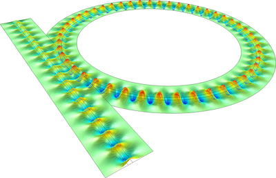
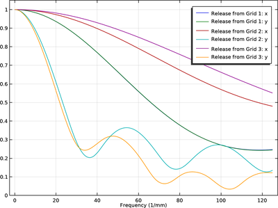
In seiner einfachsten Form besteht ein optischer Ringresonator aus einem geraden Wellenleiter und einem Ringwellenleiter. Die Wellenleiter sind nahe beieinander platziert, so dass das Licht jeweils auf die beiden Strukturen einwirkt. Wenn die Ausbreitungslänge um den Ring eine ganze ... Mehr lesen

This model demonstrates how to use topology optimization with milling constraints to design a metalens that focuses a single wavelength to a point. This involves transferring the optimized results to another component so the result can be verified using an explicit geometry ... Mehr lesen