Modeling of Complex Physics Speeds Chip Development
P. WoytowitzLam Research Corporation, CA, USA
With technological advancements accelerating so rapidly, more powerful computer chips are needed to meet the high demands of fast-growing industries. Lam Research Corporation manufactures semiconductor devices and equipment used to deposit, etch, and clean material layers laid onto wafers during semiconductor processing. With processes as precise as chemical vapor deposition (CVD), temperature fluctuations and thermal cycling can lead to defects in the deposition, selective removal, and patterning that are central to the manufacturing process.
Peter Woytowitz, director of engineering at Lam, has used COMSOL Multiphysics to understand how defects happen during manufacturing, and how wafer deformations correlate to overlay errors and misalignments. His team has designed a heating system for more uniform temperature control and simulated buckling in the temporary structures used for creating high-aspect ratio features. Using their results, they have been able to optimize their tool's performance, precisely match the degree of wafer displacement to overlay errors, and accurately predict buckling.
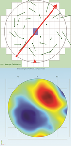 Top: a map of vectors contributing to wafer bow, resolved into wafer displacement contour maps. Bottom: view in the XY plane.
Herunterladen
- LAM_Research_Corporation_MS2014.pdf - 0.55MB