
Besi Improved Memory Chip Manufacturing with Multiphysics Simulation
Stefan Behler, Besi, Switzerland
As memory chips become smaller and smaller, designers must ensure that the chips stay intact during the manufacturing process. Besi develops equipment and assembly processes for substrate and wafer packaging production in markets such as consumer electronics, automotive, industrial, and solar energy. Stefan Behler, a senior expert process engineer, used multiphysics simulation to explore and optimize a new way of peeling off the tape on a memory chip that results in less deformation of the dies. This new method is now used by semiconductor packaging factories all over the world.
Suggested Stories
Optimierung von Messwandlern und Sensoren mit Multiphysik-Simulation
Stromnetze müssen ordnungsgemäß gewartet werden, um sie vor Systemausfällen zu schützen. Die Ingenieure von ABB ...

Simulation-Based Design of New Implantable Hearing Device
Cochlear Technology Centre Europe (CTCE) develops new technology for hearing implants. Their current work is with a ...
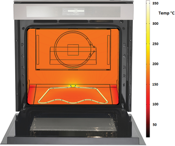
Simulation Turns Up the Heat and Energy Efficiency at Whirlpool Corporation
Engineers working on a joint research project between Whirlpool Corporation and the European initiative GREENKITCHEN ...

Upgrading the Nuts and Bolts of the Electrical Grid for a New Generation
Migrating the electrical grid to a “smart grid” is usually discussed in terms of IT issues or embedded systems. Yet, ...


