
Besi Improved Memory Chip Manufacturing with Multiphysics Simulation
Stefan Behler, Besi, Switzerland
As memory chips become smaller and smaller, designers must ensure that the chips stay intact during the manufacturing process. Besi develops equipment and assembly processes for substrate and wafer packaging production in markets such as consumer electronics, automotive, industrial, and solar energy. Stefan Behler, a senior expert process engineer, used multiphysics simulation to explore and optimize a new way of peeling off the tape on a memory chip that results in less deformation of the dies. This new method is now used by semiconductor packaging factories all over the world.
Suggested Stories
Erfüllung von Qualitätsstandards in der Öl- und Gasförderung mit Ultraschallwandlern
Baker Hughes erzielt eine Einsparung von 30 % bei den Prototypenentwicklungskosten durch den Einsatz von 3D ...
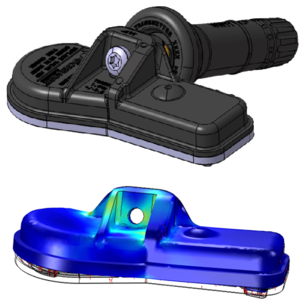
Optimizing Built-in Tire Pressure Monitoring Sensors
Built-in tire pressure sensors need to be able to withstand the wear and tear of working within a car’s tire rim. ...
A STEP in the Right Direction: Modeling AC Losses in a Tokamak Design
The Spherical Tokamak for Energy Production (STEP) program aims to deliver a prototype fusion energy plant in the ...

Ein 3D-Modell unterstützt Wissenschaftler bei der Vorhersage des thermischen Verhaltens des Mondes
Forscher des Physical Research Laboratory haben ein einzigartiges thermophysikalisches Modell entwickelt, um das ...


