
Besi Improved Memory Chip Manufacturing with Multiphysics Simulation
Stefan Behler, Besi, Switzerland
As memory chips become smaller and smaller, designers must ensure that the chips stay intact during the manufacturing process. Besi develops equipment and assembly processes for substrate and wafer packaging production in markets such as consumer electronics, automotive, industrial, and solar energy. Stefan Behler, a senior expert process engineer, used multiphysics simulation to explore and optimize a new way of peeling off the tape on a memory chip that results in less deformation of the dies. This new method is now used by semiconductor packaging factories all over the world.
Suggested Stories
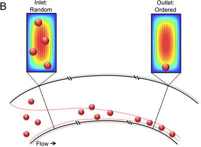
Modeling Inertial Focusing in Straight and Curved Microfluidic Channels
In many medical procedures and tests, it is necessary to isolate cells of interest for further analysis. Microfluidics ...
Investigating Intrabody Communication for Leadless Cardiac Pacemakers
MicroPort CRM used numerical simulation to optimize leadless cardiac pacemaker (LCP) designs and how they communicate ...
Generatives Design für die Entwicklung von Wasserstoff-Brennstoffzellen
Das Toyota Research Institute of North America (TRINA) arbeitet an wasserstoffbetriebenen Fahrzeugen. Das TRINA-Team ...
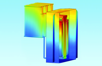
Simulation Enables the Next Generation of Power Transformers and Shunt Reactors
From power generation to its distribution to end users, power transformers and shunt reactors are used throughout the ...


