COMSOL News
Multiphysics Simulation: An IEEE Spectrum Insert
Peeling Away Memory Chips
Stefan Behler, Besi, SwitzerlandAs memory chips become smaller and smaller, designers must ensure that the chips stay intact during the manufacturing process. Besi develops equipment and assembly processes for substrate and wafer packaging production in markets such as consumer electronics, automotive, industrial, and solar energy. Stefan Behler, a senior expert process engineer, used multiphysics simulation to explore and optimize a new way of peeling off the tape on a memory chip that results in less deformation of the dies. This new method is now used by semiconductor packaging factories all over the world.
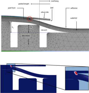 Simulation of how a chip would bend under certain operating conditions. Top: Mesh of the geometry of a memory chip. Bottom: Stress in the vertical direction of the chip.
Herunterladen
- Besi_MS2017.pdf - 2.53MB