Electroplating of a Printed Circuit Board
Application ID: 20331
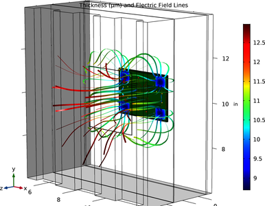
This example simulates electroplating of a printed circuit board (PCB) in 3D using the Secondary Current Distribution interface. In order to achieve thickness uniformity across the PCB, a dummy pattern is included in the design, along with an aperture in the electroplating bath.
Dieses Beispiel veranschaulicht Anwendungen diesen Typs, die mit den folgenden Produkten erstellt wurden:
Allerdings können zusätzliche Produkte erforderlich sein, um es vollständig zu definieren und zu modellieren. Weiterhin kann dieses Beispiel auch mit Komponenten aus den folgenden Produktkombinationen definiert und modelliert werden:
- COMSOL Multiphysics® und
- ECAD Import Module und
- entweder Battery Design Module, Corrosion Module, Electrochemistry Module, Electrodeposition Module, oder Fuel Cell & Electrolyzer Module
Die Kombination von COMSOL® Produkten, die für die Modellierung Ihrer Anwendung erforderlich ist, hängt von verschiedenen Faktoren ab und kann Randbedingungen, Materialeigenschaften, Physik-Interfaces und Bauteilbibliotheken umfassen. Bestimmte Funktionen können von mehreren Produkten gemeinsam genutzt werden. Um die richtige Produktkombination für Ihre Modellierungsanforderungen zu ermitteln, lesen Sie die Spezifikationstabelle und nutzen Sie eine kostenlose Evaluierungslizenz. Die COMSOL Vertriebs- und Support-Teams stehen Ihnen für alle Fragen zur Verfügung, die Sie diesbezüglich haben.