Die Application Gallery bietet COMSOL Multiphysics® Tutorial- und Demo-App-Dateien, die für die Bereiche Elektromagnetik, Strukturmechanik, Akustik, Strömung, Wärmetransport und Chemie relevant sind. Sie können diese Beispiele als Ausgangspunkt für Ihre eigene Simulationsarbeit verwenden, indem Sie das Tutorial-Modell oder die Demo-App-Datei und die dazugehörigen Anleitungen herunterladen.
Suchen Sie über die Schnellsuche nach Tutorials und Apps, die für Ihr Fachgebiet relevant sind. Beachten Sie, dass viele der hier vorgestellten Beispiele auch über die Application Libraries zugänglich sind, die in die COMSOL Multiphysics® Software integriert und über das Menü File verfügbar sind.
This model shows how to set up a 3D simulation of a n-p-n bipolar transistor. It is a 3D version of the device shown in the Bipolar Transistor model, and demonstrates how to extend semiconductor modeling into 3D using COMSOL Multiphysics. As in the 2D version of this model, the device ... Mehr lesen

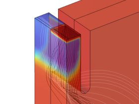
This benchmark example builds two models of a cross-bridge Kelvin resistor used for extracting the specific contact resistivity. The first model simulates the system in 3D, using the contact resistance feature built in the Semiconductor interface. The other model is a 2D approximation of ... Mehr lesen
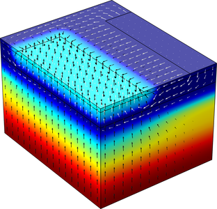
In this second half of a two-part example, a 3D model of a trench-gate IGBT is built by extruding the 2D model from the first half. Unlike the 2D model, now it is possible to arrange the alternating n+ and p+ emitters along the direction of extrusion as in the real device. This more ... Mehr lesen
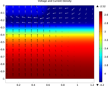
This model shows how to set up a simple Bipolar Transistor model. The output current-voltage characteristics in the common-emitter configuration are computed and the common-emitter current gain is determined. Mehr lesen

This tutorial performs steady-state and transient analysis of the response of a PIN diode to constant and pulsed radiation, respectively. The effect of radiation is modeled as spatially uniform generation of electron-hole pairs within the device. At high dose rates the separation of the ... Mehr lesen

This model shows how to model the avalanche breakdown due to the impact ionization in a Silicon Carbide diode. The current-voltage (I-V) characteristics of the device are presented as well as the electric field distribution plot. Furthermore, the carrier generation term has been computed ... Mehr lesen

This model demonstrates how to couple the Semiconductor interface to the Heat Transfer in Solids interface. A thermal analysis is performed on the existing bipolar transistor model in the case when the device is operated in the active-forward configuration. The Semiconductor interface ... Mehr lesen
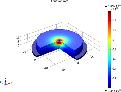
This model simulates an LED that emits in the infrared part of the electromagnetic spectrum. The device structure is made up of a single p-n junction formed by a layer of p-type doping near the top surface of an otherwise n-type wafer. This kind of device geometry is simple and cheap to ... Mehr lesen

This model extracts spice parameters for a silicon p-n junction diode. The spice parameters are used to create a lumped-element equivalent circuit model of a half-wave rectifier that is compared to a full device level simulation. In this example, a device model is made by connecting a 2D ... Mehr lesen

This tutorial demonstrates the use of the density-gradient formulation to include the effect of quantum confinement in the device physics simulation of a silicon inversion layer. This formulation requires only a moderate increase of computational resources as compared to the conventional ... Mehr lesen