3D-Printed Microfluidic Chip System for Dielectrophoretic Manipulation of Colloids
INTRODUCTION:
Microfluidics, as a crucial technology of recent years, enables numerous applications for Point-of-Care-Testing such as Lab-on-Chip-Systems (LOC) or Micro-Total-Analysis-Systems (µTAS) and is exceptionally well-suited for cell sorting or DNA trapping. Especially the implementation of dielectrophoresis (DEP) in microfluidic systems has evolved to a subtle method for precise manipulation of appropriate cells, molecules or particles [1,2].
DEP is based on the movement of particles in a non-uniform electric field due to the interaction between the dipole of the particle and the spatial gradient of the electric field. Thereby, the generated dielectrophoretic force depends on two main parameters, the particle size and the electrical properties of the suspending medium [3,4]. In this context, the aforementioned force is responsible for deflection of particles in microfluidic channels and leads to characteristic trajectories of the colloids within these filigree structures [5].
To investigate DEP, an additive manufactured chip system was developed. Contrary to conventional production methods, additive manufacturing, also known as 3D-printing, allows the generation of sophisticated microscale channel geometries and represents a relatively simple and inexpensive alternative for prospective production of such systems [6]. To ensure the formation of a non-uniform electric filed, the integration of electrodes inside the device is mandatory. The FEM-model reported in this work is used for finding an optimized electrode design as well as operation conditions.
USE OF COMSOL Multiphysics®:
The model is set up with the Electrostatics interface, the Laminar Flow interface and the Particle Tracing module. For numeric efficiency, a 2D geometry of the channel system is established in order to simulate the deflection of particles due to the dielectrophoretic force caused by an electric DC-field.
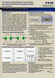
RESULTS:
Figure 1 illustrates the result of the simulation and the chip. As expected, the particles were deviated into the bottom outflow branch under the influence of the electric DC-field due to the biased arrangement of electrodes and the generation of dielectrophoretic force.
CONCLUSION:
Using the Electrostatics interface, the Laminar Flow interface as well as the Particle Tracing module, a model was set up to investigate the functionality of a microfluidic chip system for dielectrophoretic manipulation of particles. The measured results provide evidence to optimize the prototype regarding the positioning of the electrodes and the applied voltage.
REFERENCES:
[1] J. Castillo-León, (Ed.): Lab-on-a-Chip Devices and Micro-Total Analysis Systems. A Practical Guide. Cham: Springer, 2015.
[2] P. K. Wong et al.: Electrokinetics in Micro Devices for Biotechnology Applications. In: IEEE/ASME Transactions on Mechatronics 9(2) (2004), pp. 366–376.
[3] H. A. Pohl: Dielectrophoresis: The Behavior of Neutral Matter in Nonuniform Electric Fields. Cambridge monographs on physics. Cambridge und New York: Cambridge University Press, 1978.
[4] T. B. Jones: Electromechanics of particles. Cambridge: Cambridge University Press, 1995.
[5] N. Lewpiriyawong, C. Yang & Y. C. Lam: Continuous sorting and separation of microparticles by size using AC dielectrophoresis in a PDMS microfluidic device with 3-D conducting PDMS composite electrodes. In: Electrophoresis 31(15) (2010), pp. 2622–2631.
[6] A. K. Au et al.: Mikrofluidik aus dem 3D-Drucker. In: Angewandte Chemie 128(12) (2016), pp. 3926–3946.
Herunterladen
- kuehne_poster.pdf - 1.36MB
- kuehne_paper.pdf - 1.57MB
- kuehne_abstract.pdf - 0.05MB