Silicon Nanopillar Array for Light Emission Enhancement in Color-converting LED
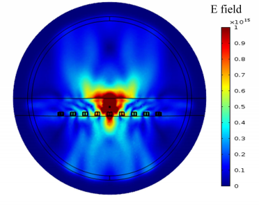
Plasmonic metallic nanostructures have been demonstrated an effective way to enhance the light emission efficiency in LEDs. Here, we propose a design of white LEDs that combining dielectric silicon nanopillar array in the color-converting layer. By investigating theoretically the guided mode caused by the nanopillar array-waveguide system, we demonstrate that the silicon nanopillar arrays enable larger near-field enhancement and more efficient photons emission property than the plasmonic counterparts [1]. These performances make the silicon nanopillar arrays have potential application in light converter for efficient white LEDs. A schematic of the proposed structure is presented in Fig. 1. The square or hexagonal Si nanopillar array is embedded in a polymer waveguide layer (n=1.59) and deposited on a glass silica substrate (n=1.46), constituting a nanoparticle array-waveguide system. In practice, the polymer layer is doped with dye molecules, rare-earth ions or QDs, acting as a color-converting layer to combine with the blue LED. For its plasmonic counterpart used for comparison, an aluminum nanopillar array is embedded in the polymer layer with the same structural parameters. Optical constants of crystalline Si and Al are taken from Palik [2]. All calculations are performed in COMSOL Multiphysics® 5.1 with the wave optics module. Optical response of the nanoparticle array-waveguide system can be obtained by simulating a unit cell in the computational domain, with Floquet periodic boundary employed for four lateral boundaries and perfectly matched layers (PML) in the vertical (z) direction. To evaluate the extinction and near-field enhancement effects of the guided modes excited in polymer layer, the system is excited by a plane wave under normal incidence. The extinction is defined as 1-T, with T being the transmittance that obtained by normalizing the output power at the top boundary to that of the background field. For the investigation of the nanopillar array-mediated emission, the unit cell is driven by a classical electric dipole at the center of the color-converting layer. The influence of the Si or Al nanoparticle arrays on the emission enhancement is computed by performing surface integrals over the Poynting vector on the upper and lower boundaries of the model in the presence and absence of the nanoparticle arrays. Due to the low-loss directional scattering of single Si nanopillar [3], the array of Si nanopillars is demonstrated to enable more significant near-field enhancement and emission enhancement than its plasmonic counterparts (see Fig.2 and 3). This makes the light-converting layer deposited over Si nanoparticle array may be an efficient light converter. The guided mode excited in light-converting can be controlled by changing the period of nanopillar grating and the layer thickness [1]. More significant near-field and far-field performance can be achieved by further optimizing the shape, size and position of Si nanoparticles. We expect our research open a new path to design and optimize the solid-state lighting systems by introducing large-area silicon nanostructures. The results also provide insights into the design of all-dielectric metamaterials for gaining or lasing devices.
Herunterladen
- ding_poster.pdf - 1.01MB
- ding_abstract.pdf - 0.53MB