
Stationary and Transient Analysis of a Planar GaAs Gunn Device Using COMSOL Multiphysics
Planar Gunn devices can generate microwave-to-terahertz oscillations through the transferred-electron effect or Gunn effect: above a threshold electric field, intervalley electron transfer produces negative differential mobility and negative differential resistance (NDR), supporting self-sustained moving high-field domains. This mechanism has been exploited across III–V material systems, including GaAs, InGaAs, InP and GaN, with operation extending from microwave frequencies towards the terahertz range [1–3]. Predicting the static NDR characteristic and the resulting transient oscillations directly from carrier-transport physics is valuable for device design but numerically demanding, since the solution is sensitive to the mobility model, device geometry, donor concentration, contact conditions, spatial discretisation, time stepping and time-dependent initialisation.
A two-dimensional lateral planar GaAs Gunn device was developed in COMSOL Multiphysics® 6.3 using the Semiconductor Module. The modelled device has a 4 µm anode–cathode gap, a 0.3 µm active layer thickness, a 60 µm width and a donor concentration of 8 × 10¹⁶ cm⁻³. Electron transport was described using the drift-diffusion equation together with a custom field-dependent mobility relation representing the negative differential mobility of GaAs. Finite specific contact resistivity was applied at the anode and cathode ohmic contacts.
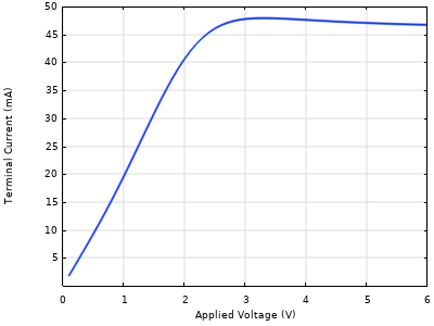
Stationary voltage sweeps were performed to study the effects of geometrical, transport and contact parameters on the current–voltage response. The stationary simulations showed that device width, active-layer thickness and donor concentration primarily control the current magnitude, whereas contact spacing and contact resistivity shift the voltage at which the high-field response occurs. Saturation velocity and the characteristic field parameter strongly influence the current peak and post-peak reduction. For the 4 µm gap device, the simulated current reached 48 mA at 3.3 V and decreased slightly to 46.5 mA at 6 V.
A time-dependent extension of the two-dimensional model was also investigated. Initial simulations produced sustained terminal-current oscillations following the voltage ramp. Further mesh and time-step sensitivity studies, together with examination of the spatial electron-density and electric-field evolution, are being undertaken to distinguish travelling-domain behaviour from contact-related or numerical fluctuations and to determine the dominant physical oscillation frequency.
The results demonstrate that device geometry, high-field transport parameters, contact treatment and numerical resolution materially affect the simulated stationary and transient response. The developed workflow provides a practical basis for progressing from stationary parameter analysis to numerically stable time-dependent modelling of planar GaAs Gunn-type devices.
Herunterladen
- 19191_final_poster.pdf - 0.81MB


