
Intel Optimizes an Electronic Device Component with Simulation
Juan C. Cervantes-Gonzalez, Intel Guadalajara Design Center, Mexico
As the demand grows for faster electronic devices in smaller packages, we need to develop optimized high-speed interconnects, which transfer the signal between components in electronic devices. Found in printed circuit boards (PCB), this integral design element in electronics packaging carries signals laterally and through the depth of PCBs, traversing many layers of metal and dielectric material. To satisfy these growing technology demands, interconnects must be designed smaller, more closely packed, and able to operate at higher frequencies.
To reduce the number of prototypes required to test new interconnect designs, engineers at the Intel Guadalajara Design Center developed an efficient computational design optimization method, combining full-wave electromagnetic simulation in COMSOL Multiphysics® software with a space-mapping (SM) algorithm implemented in MATLAB® software. Through their approach, an interconnect design can be quickly optimized, streamlining the design cycle and time to market of the latest high-speed interconnect technology.
Suggested Stories
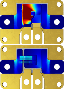
Innovative Packaging Design for Electronics in Extreme Environments
Power electronics appear in many everyday products, including smartphones, electronic car parts, and household ...
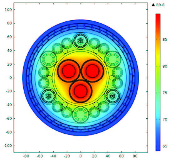
Simulation Software Brings Big Changes to Cable Industry
The design and testing of high-voltage cables for terrestrial and submarine applications is paramount to Prysmian's ...
Simulation-Led Strategy for Corrosion Prevention
Corrosion is a widespread concern costing the US billions of dollars annually. For the Navy, specifically, it is the ...
Sea Floor Energy Harvesting
Veryst Engineering has provided design solutions for a variety of industries in the field of energy harvesting. One of ...


