
Besi Improved Memory Chip Manufacturing with Multiphysics Simulation
Stefan Behler, Besi, Switzerland
As memory chips become smaller and smaller, designers must ensure that the chips stay intact during the manufacturing process. Besi develops equipment and assembly processes for substrate and wafer packaging production in markets such as consumer electronics, automotive, industrial, and solar energy. Stefan Behler, a senior expert process engineer, used multiphysics simulation to explore and optimize a new way of peeling off the tape on a memory chip that results in less deformation of the dies. This new method is now used by semiconductor packaging factories all over the world.
Suggested Stories
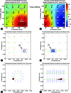
Multiphysics Simulations Help Track Underground Fluid Movements
Combining acoustic and electromagnetic analyses helps scientists to more efficiently measure and survey subterranean ...
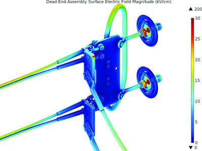
Enhancing Transmission Line Performance: Using Simulation to Optimize Design
Designing power transmission lines requires accounting for many factors: mechanical stress due to environmental ...
Analyzing the LHC Magnet Quenches
Engineers and physicists at CERN go to great lengths to ensure that the high-power superconducting magnets that ...
Industrial Applications of Carbon and Graphite for Thermal Management
At GrafTech International, engineers develop carbon and graphite products for applications from consumer electronics ...


