
Besi Improved Memory Chip Manufacturing with Multiphysics Simulation
Stefan Behler, Besi, Switzerland
As memory chips become smaller and smaller, designers must ensure that the chips stay intact during the manufacturing process. Besi develops equipment and assembly processes for substrate and wafer packaging production in markets such as consumer electronics, automotive, industrial, and solar energy. Stefan Behler, a senior expert process engineer, used multiphysics simulation to explore and optimize a new way of peeling off the tape on a memory chip that results in less deformation of the dies. This new method is now used by semiconductor packaging factories all over the world.
Suggested Stories
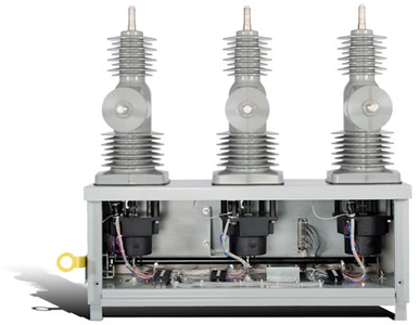
How Reclosers Ensure a Steady Supply of Power: It’s All in the Magnet
When a tree branch touches overhead cables and causes a momentary short circuit, your lights may flicker. A device ...
Shaping the Design of Noninvasive Cosmetic Procedures with Multiphysics Simulation
Allergan Aesthetics is using heat transfer and electromagnetics simulation to enhance CoolSculpting® and CoolTone®, ...
Improving Efficiency in Iron Ore Sintering
VDEh-Betriebsforschungsinstitut (BFI) is one of Europe’s leading research institutions in the development of iron- and ...
Conjugate Heat Transfer
This is an application brief describing the concept of Conjugate Heat Transfer, which is important in many industrial ...


