
Besi Improved Memory Chip Manufacturing with Multiphysics Simulation
Stefan Behler, Besi, Switzerland
As memory chips become smaller and smaller, designers must ensure that the chips stay intact during the manufacturing process. Besi develops equipment and assembly processes for substrate and wafer packaging production in markets such as consumer electronics, automotive, industrial, and solar energy. Stefan Behler, a senior expert process engineer, used multiphysics simulation to explore and optimize a new way of peeling off the tape on a memory chip that results in less deformation of the dies. This new method is now used by semiconductor packaging factories all over the world.
Suggested Stories
Life-Science-Unternehmen beschleunigt die biopharmazeutische Forschung und Entwicklung mit einer dedizierten CAE-Abteilung
Die Entwicklung von Biopharmazeutika ist aufgrund ihrer komplexen molekularen Struktur, der dafür erforderlichen ...
Defying Convention to Achieve Faster Signal and Simulation Speeds
As the demand grows for faster electronic devices in smaller packages, we need to develop optimized high-speed ...
Increasing Lifespans of High-Power Electrical Systems
ABB Semiconductors increased the lifespan of an insulated-gate bipolar transistor (IGBT) using multiphysics ...
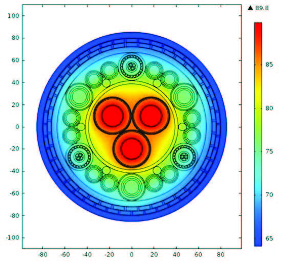
Simulation Software Brings Big Changes to Cable Industry
The design and testing of high-voltage cables for terrestrial and submarine applications is paramount to Prysmian's ...


