Die Application Gallery bietet COMSOL Multiphysics® Tutorial- und Demo-App-Dateien, die für die Bereiche Elektromagnetik, Strukturmechanik, Akustik, Strömung, Wärmetransport und Chemie relevant sind. Sie können diese Beispiele als Ausgangspunkt für Ihre eigene Simulationsarbeit verwenden, indem Sie das Tutorial-Modell oder die Demo-App-Datei und die dazugehörigen Anleitungen herunterladen.
Suchen Sie über die Schnellsuche nach Tutorials und Apps, die für Ihr Fachgebiet relevant sind. Beachten Sie, dass viele der hier vorgestellten Beispiele auch über die Application Libraries zugänglich sind, die in die COMSOL Multiphysics® Software integriert und über das Menü File verfügbar sind.

Dieses einfache Modell zeigt, wie Sie die Interfaces Semiconductor Optoelectronics verwenden können, um eine einfache GaAs-PIN-Diodenstruktur zu modellieren. Sowohl die stimulierte als auch die spontane Emission im Halbleiter werden berücksichtigt. Die entsprechende Absorption des Lichts ... Mehr lesen
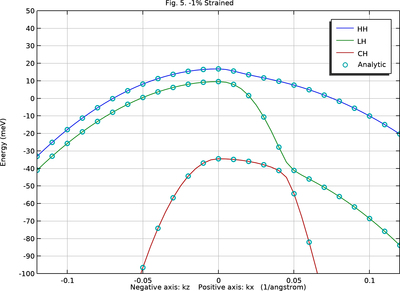
This benchmark model computes the valence band structure of an unstrained and a strained bulk GaN wurtzite crystal, as a tutorial for users who wish to set up multiple wave function components with the Schrödinger Equation interface. The model follows the formulation given in the ... Mehr lesen
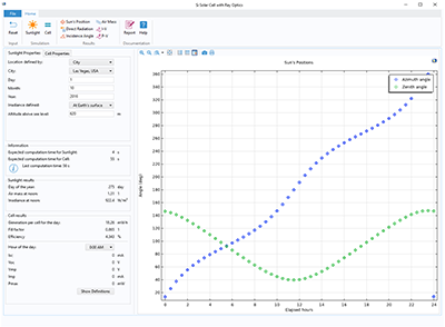
This app demonstrates the following: Multiple components (1D and 3D) in a single app Using the same choice list in the app as in the model using Data Access functionality Output numerical results for a specific time step using a combo box The app combines the Ray Optics Module and ... Mehr lesen

In this first half of a two-part example, a 2D model of a trench-gate IGBT is built, which will be extended to 3D in the second half. In general, it is the most efficient to start with a 2D model to make sure everything works as expected, before extending it to 3D. The Caughey&ndash ... Mehr lesen

The metal-silicon-oxide (MOS) structure is the fundamental building block for many silicon planar devices. Its capacitance measurements provide a wealth of insight into the working principles of such devices. This tutorial constructs a simple 1D model of a MOS capacitor (MOSCAP). Both ... Mehr lesen
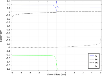
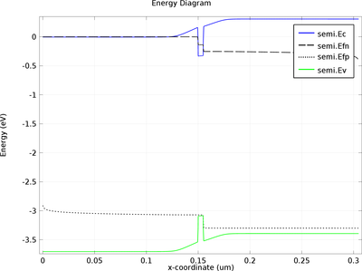
In a diode or a transistor, when a p-n junction is reverse-biased (the p-side is connected to a lower potential than the n-side), ideally, no current should flow. However, due to minority carriers (electrons in the p-side and holes in the n-side), a small current, known as the reverse ... Mehr lesen

MOSFETs typically operate in three regimes depending on the drain-source voltage for a given gate voltage. Initially the current-voltage relation is linear, this is the Ohmic region. As the drain-source voltage increases the extracted current begins to saturate, this is the saturation ... Mehr lesen
This benchmark model simulates three different heterojunction configurations under forward and reverse bias. It shows the difference in using the continuous quasi-Fermi level formulation versus the thermionic emission formulation for the charge transfer across the heterojunction. The ... Mehr lesen
This model simulates a GaN based light emitting diode. The emission intensity, spectrum, and quantum efficiency are calculated as a function of the driving current. Direct radiative recombination across the band gap is modeled, as well as non-radiative Auger and trap-assisted ... Mehr lesen

The double barrier structure is of interest because of its application in semiconductor devices such as resonant-tunneling diodes. This verification example demonstrates the Schrödinger Equation interface to set up a simple 1D GaAs/AlGaAs double barrier structure to analyze the ... Mehr lesen