Neuerungen im Semiconductor Module
Für Nutzer des Semiconductor Module bietet COMSOL Multiphysics® Version 6.4 eine vereinfachte Modellierung ferroelektrischer und piezoelektrischer Halbleiter, einen optimierten Workflow für die Simulation neuartiger Halbleiterarchitekturen, die Möglichkeit, optische Übergänge direkt aus den optischen Materialeigenschaften zu definieren und vieles mehr. Weitere Informationen zu diesen Updates finden Sie unten.
Multiphysik-Feature Semiconductor–Electrostatics Coupling
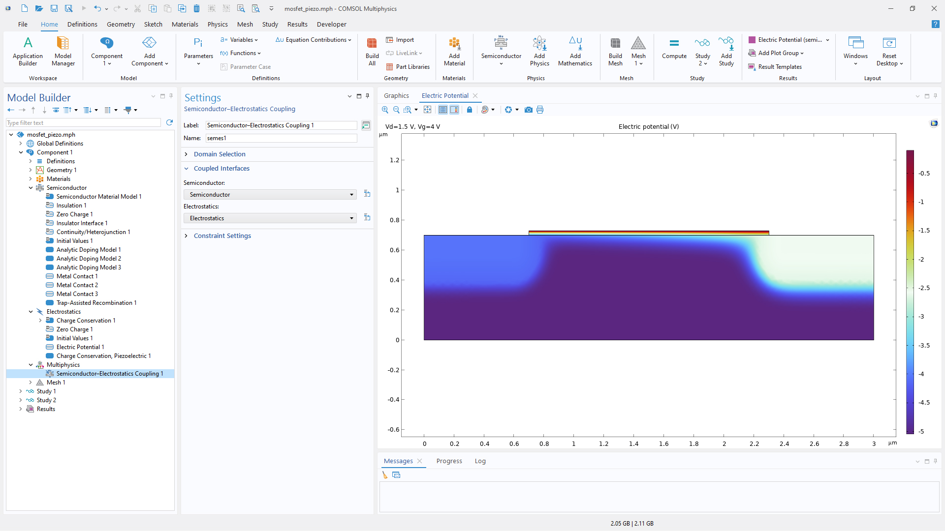
Bei der Simulation ferroelektrischer und piezoelektrischer Halbleiter kann das neue Multiphysik-Feature Semiconductor–Electrostatics Coupling verwendet werden, wenn eine erweiterte elektrostatische Formulierung – wie beispielsweise Charge Conservation, Ferroelectric – erforderlich ist. Diese Funktion überschreibt die im Interface Semiconductor definierte integrierte elektrostatische Gleichung und ersetzt sie durch eine in einem separaten Interface Electrostatics definierte Gleichung. Diese erweiterten Formulierungen können je nach den verwendeten Features zusätzliche Add-On-Produkte erfordern, wie beispielsweise das AC/DC Module.
Multiphysikalische Modellierung neuartiger Halbleiterarchitekturen
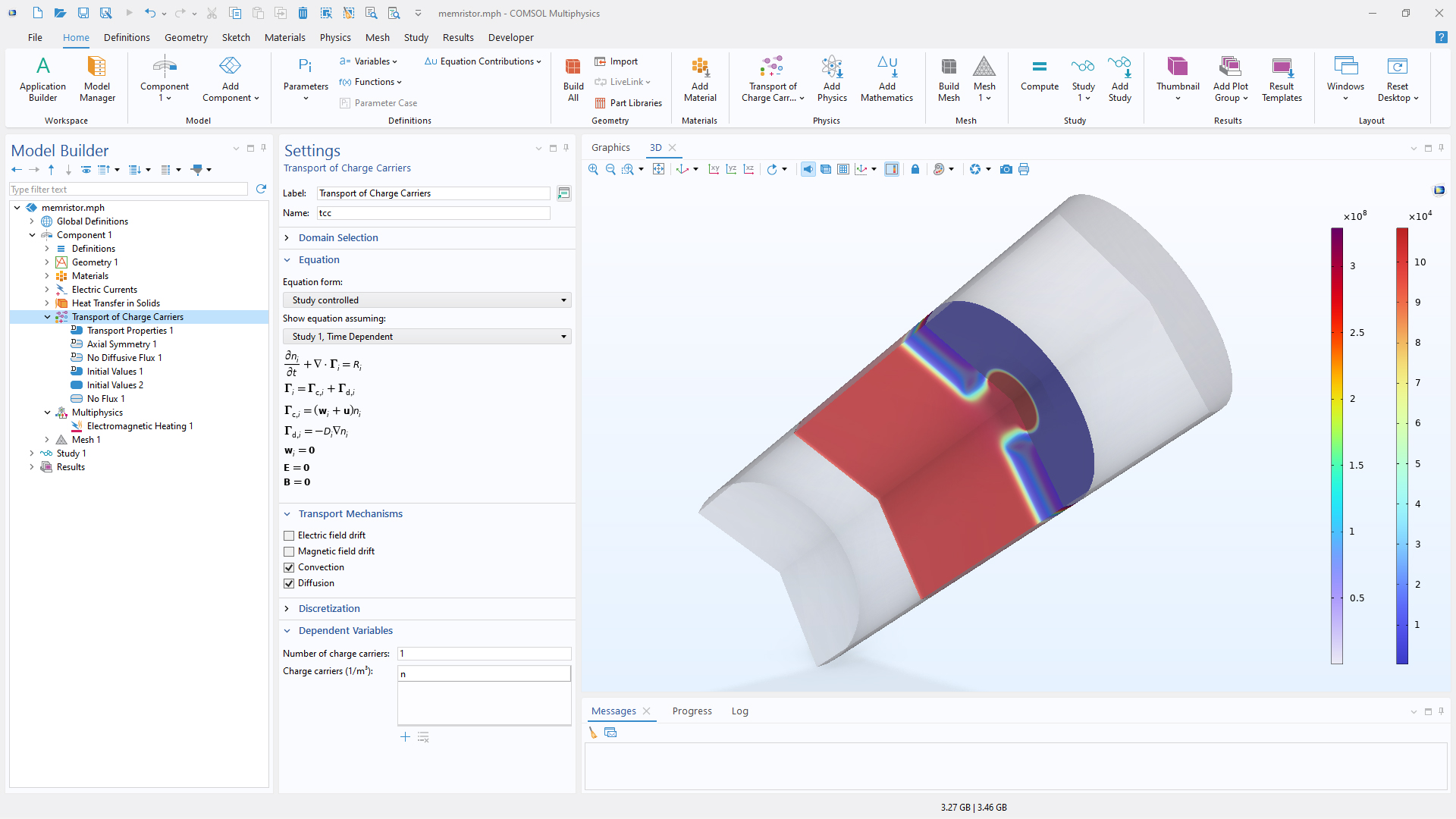
Für die Modellierung neuartiger Halbleiterarchitekturen, bei denen häufig spezielle Ladungstransportmodelle in Verbindung mit mehreren anderen physikalischen Phänomenen erforderlich sind, ermöglicht das Interface Transport of Charge Carriers im Semiconductor Module die nahtlose Integration von benutzerdefinierten Ladungsträgertransportmodellen in thermische und elektromagnetische Simulationen. Erkunden Sie diesen Multiphysik-Modellierungs-Workflow im Tutorial-Modell Memristor.
Neues Modell in Indirect Optical Transitions
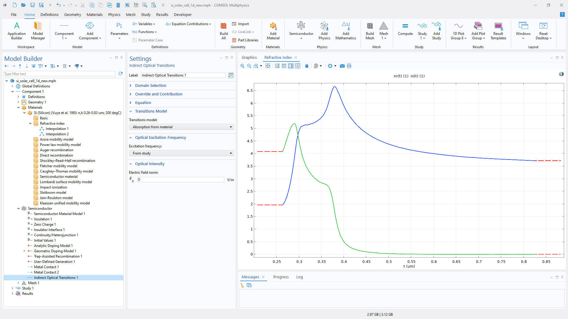
Um optische Übergänge direkt aus optischen Materialien definieren zu können, führt das Feature Indirect Optical Transitions ein neues Modell ein, bei dem der Brechungsindex des Materials zur Berechnung der indirekten Absorptionserzeugungsrate verwendet wird.
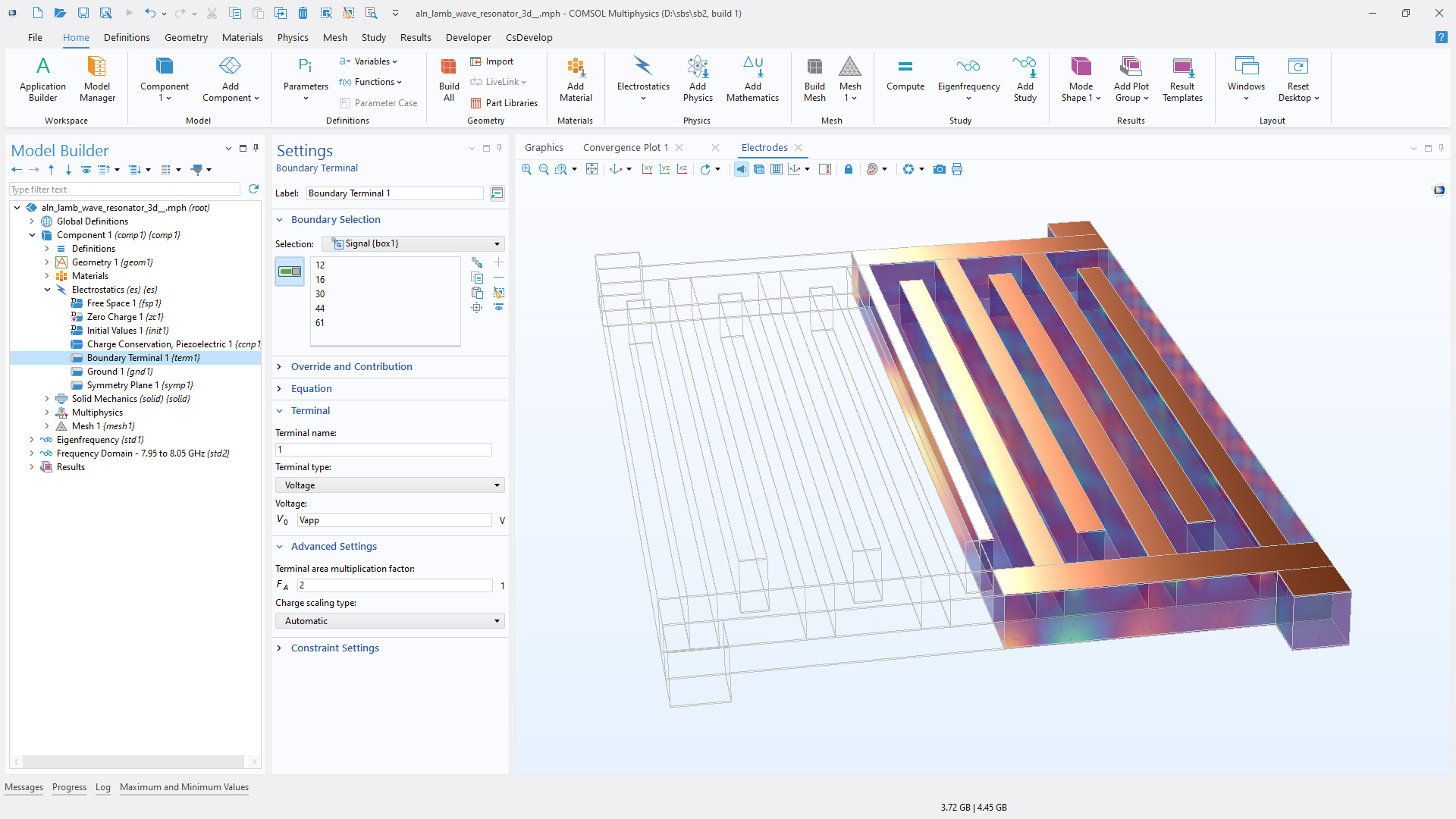
Symmetrie für Terminal
Das Feature Terminal unterstützt nun einen Flächenmultiplikationsfaktor (verfügbar im Abschnitt Advanced Settings nach Aktivierung der Advanced Physics Options). Dieser berücksichtigt die Symmetrie, indem er die Terminalfläche skaliert, sodass verbundene Schaltungen oder Lasten das gesamte Gerät erkennen, auch wenn nur ein Teil modelliert ist. Beispielsweise sollte ein Faktor von 2 verwendet werden, wenn das Modell die Hälfte des Geräts darstellt. Das Update ist für die Interfaces Electrostatics, Electric Currents und Magnetic and Electric Fields verfügbar.
Aktualisierte Tutorial-Modelle
COMSOL Multiphysics® Version 6.4 enthält die folgenden aktualisierten Tutorial-Modelle für das Semiconductor Module.
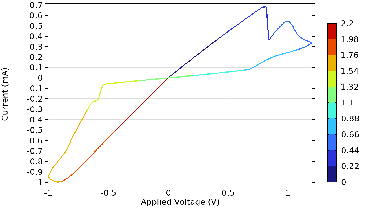
Memristor
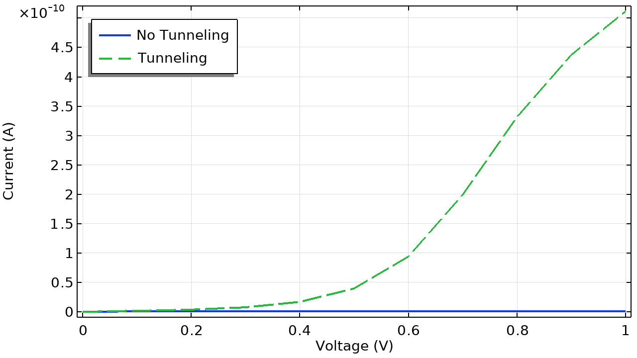
Metal–Insulator–Metal (MIM) Diode
Shockley Diode

Tunnel Diode